| The Commodore Plus/4 is a weird little machine. Although the hardware for the NTSC and PAL versions of this computer are nearly the same, there is a substantial library of software for this computer which only runs properly on one or the other variant. For this reason, it is desirable to be able to switch a machine back and forth between PAL and NTSC modes, to be capable of running any software. |
Part Quantity Supplier Part Number --------------------------------------------------------- XTAL 17.734475 18PF 1 Digi-key 300-8503-ND DPDT sliding switch 1 Digi-key CKN10034-ND 22pf capacitor 1 10k ohm resistors 2 |
|
The following tools are required: soldering iron, desoldering pump (if you
make a mistake), screwdrivers, wire cutters, pliers, drill, and a heat gun.
There are other miscellaneous materials which are necessary to build this mod, including: heat-shrink tubing, solder, flux, flux remover, small jumper wire, and screws. |
| Here's the Plus/4 motherboard: |
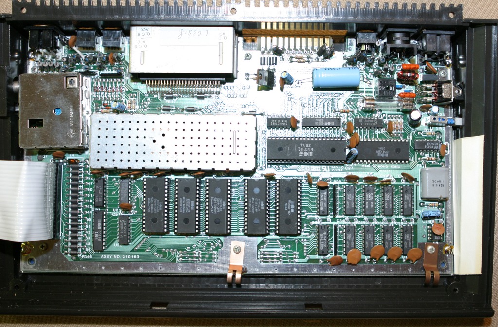
| This mod requires us to switch two different signal paths depending upon the output video mode (NTSC or PAL). The first thing we must switch is the system clock crystal. This crystal is 14.318181MHz for an NTSC machine, but 17.734475MHz for a PAL machine. In the center of this board, there is a high-frequency cage (it has a tin lid with holes drilled in it on a grid). The 8360 TED display/sound chip is in here, and the crystal is in the lower left corner. Pry the lid off carefully (it might take a lot of force). |
|
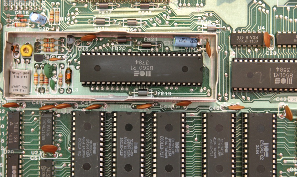
Before I started the mod, I wanted to measure the oscillator frequency of the stock system. I tried my DVM but apparently 14 MHz is beyond its range. So I used an oscilloscope to look at the signal on pin 14 of the 8360 chip: |
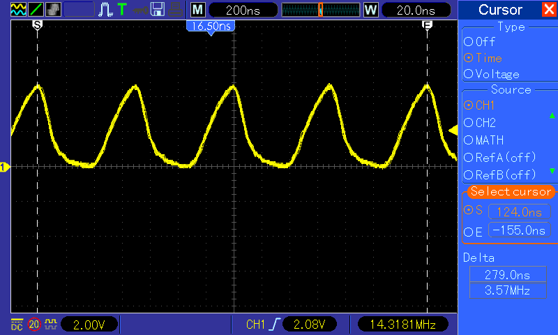
| As you can see, I measured 4 cycles at 279.0ns. The scope also prints the fundamental frequency of the input signal, and it gives 14.3181MHz, which is exactly correct for NTSC. |
|
Heat up the right most solder pad where the crystal is connected and pull the wire upwards with needle-nose pliers to pull it out of the PCB. Bend it straght up. Position the DPDT switch near its final position and measure out two wires to connect between the switch and the crystal. The wire connecting to the center bottom terminal of the switch should go into the PCB where the crystal was previously connected. The wire connecting to the left bottom terminal of the switch should go to the crystal's newly detached lead. I started with an NTSC machine, so the original NTSC crystal will be used when the switch is pulled towards the user (which is to the left when looking at the switch from the back).
I temporarily connected the right leg of the lower switch pole to the PAL crystal for testing. I got a 17.734475MHz crystal from digi-key and several different small capacitors at Fry's. You need to use a capacitor which has the right value in order to correctly balance the oscillator circuit. Each crystal has a characteristic value called load capacitance (CL), and you need to choose a capacitor to give a load capacitance in the circuit which closely matches the value for the crystal. The actual CL of the circuit is given as the series combination of the capacitors on each side of the crystal. One side is fixed by components on the motherboard, and is close to to 89pf. The other side is given by the capacitor that you choose to install with the crystal. The Plus/4 schematics give a CL of 32pf for the NTSC crystal, but the digi-key crystal that I bought for PAL has a CL value of 18pf. The equation to calculate the capacitor value is: (89 * CL) / (89 - CL). So I used a 22pf capacitor to go with the PAL crystal. As you can see from the picture below, one leg of the crystal connects to the right terminal of the lower pole of the switch. The other leg of the crystal connects to the capacitor, and the other leg of the capacitor goes to ground. |
| With this test setup and the switch in the 'PAL' position (towards the back of the computer), I observed the following signal on pin 14 of the 8360 TED chip: |
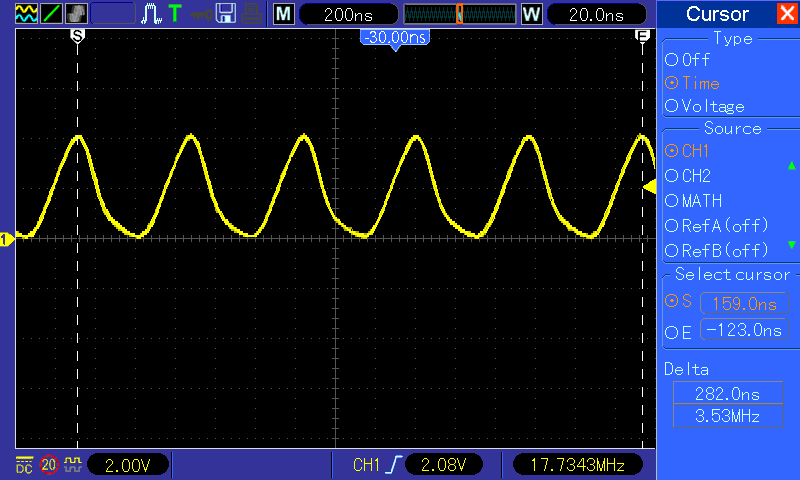
| I measured 5 cycles in 282.0ns, and the scope showed a frequency of 17.7343MHz. This looks great, so I decided to mount the switch and solder in the PAL crystal. |
| In order to mount the switch, I took an extra one and used a gold sharpie to mark 4 lines: the centers of the 2 outer mounting holes, and the outer limits of the center hole which accommodates the moving switch piece. |
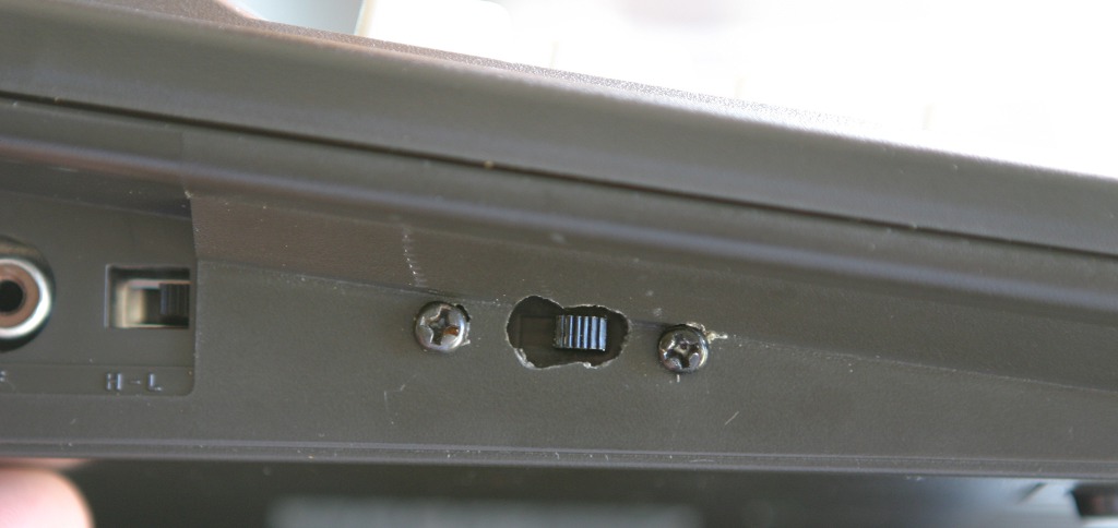
| First, drill from the inside of the case to the outside with a very small bit (5/64" or 1/16") using a dremel or small drill. Then use a bigger bit and/or reamer to open up the holes from outside going in, making sure to cut the holes level and straight. Here's what it looked like after cutting the holes open: |
| And here is the switch mounted in the case (I know, my dremel skills are lacking): |
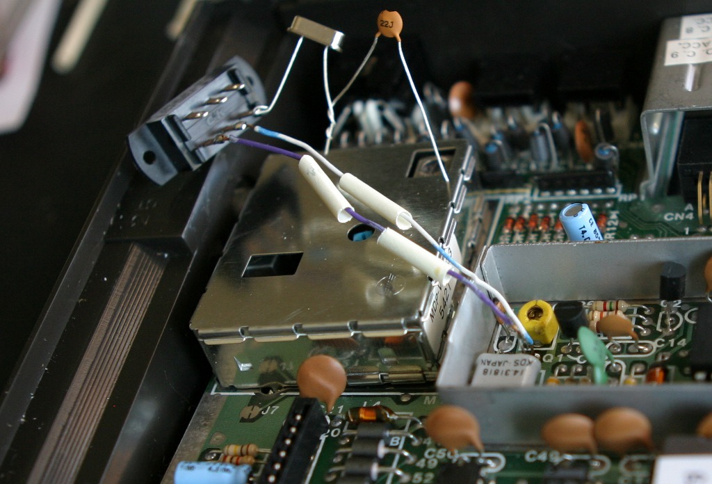
| After the switch is mounted, carefully bend the leads of the crystal and capacitor at right angles, trim them short, and then twist and solder the leads together with the switch. Solder a piece of small (30 gauge) hook-up wire to the free capacitor lead. Cut heat shrink tubing to cover the switch lug, crystal, and capacitor. Solder the hookup wire to a suitable ground. I used the left side of R15: |
| When the soldering is all done and the connections are tested, route the wires nicely, put all the pieces of heat-shrink tubing in place, and shrink them. Here is the first (crystal) part of the mod, completed: |
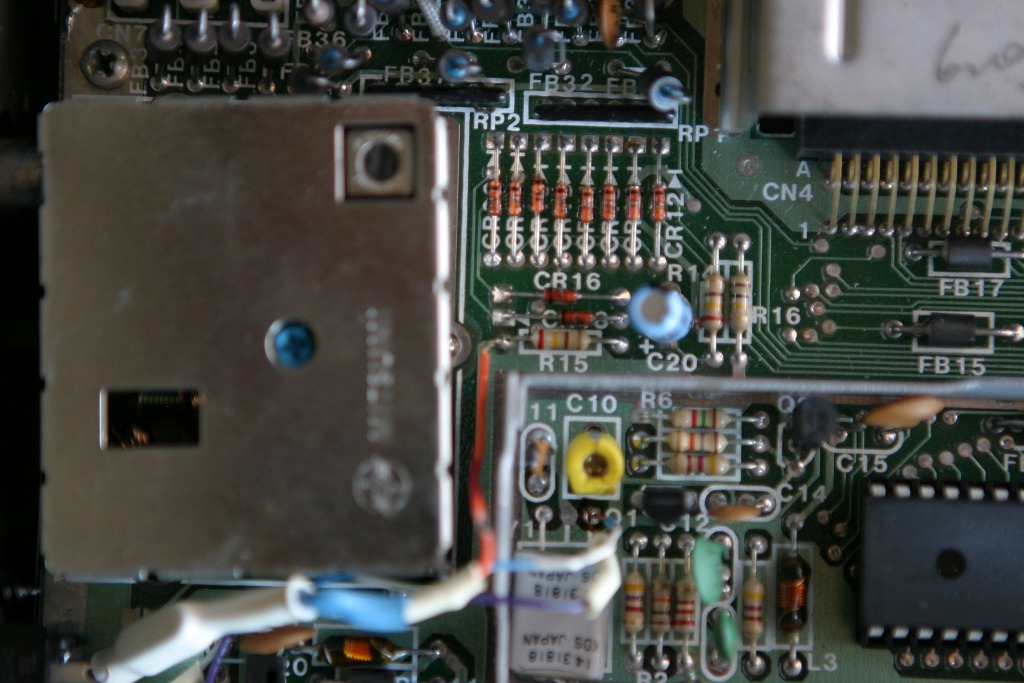
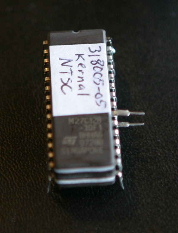
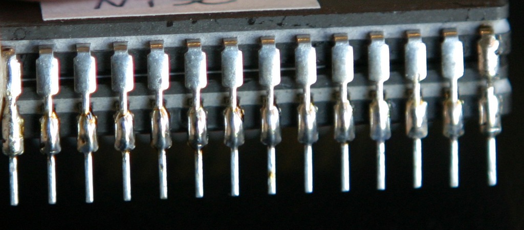
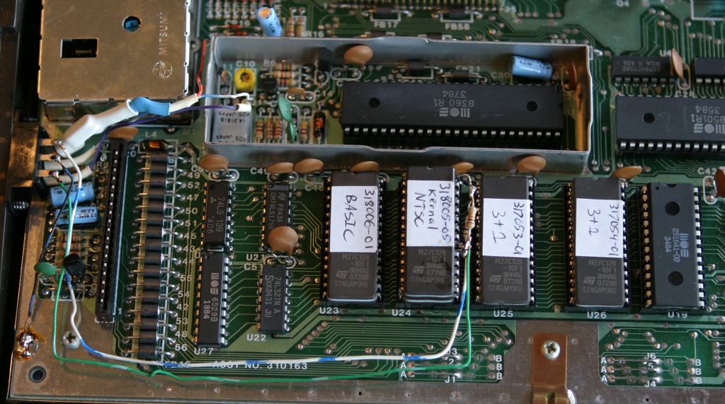
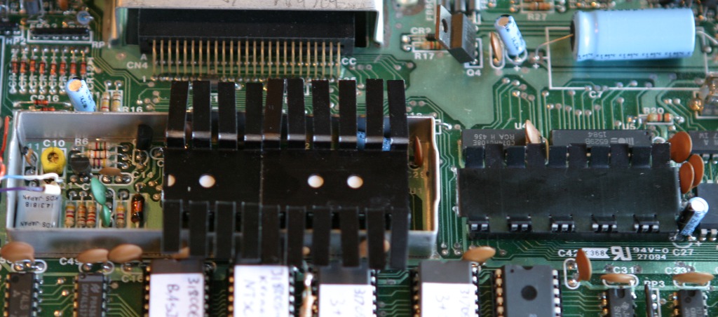
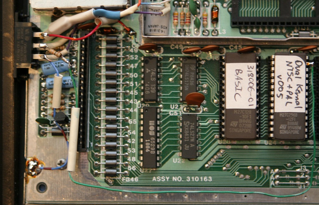
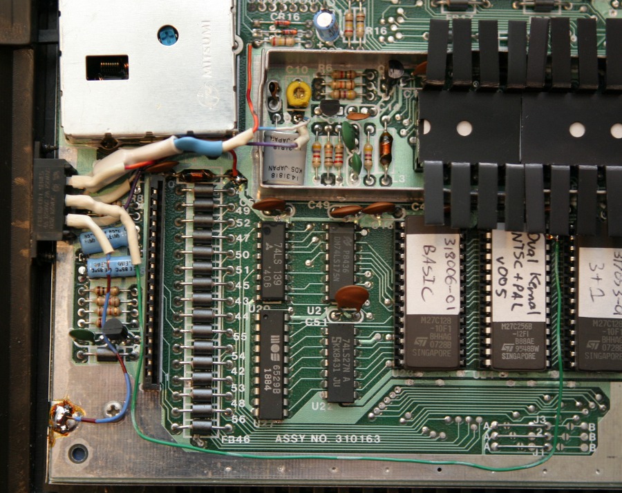
| The second half of the switch (the top pole) changes the kernal ROM. In the lower half of the board, there are five 28-pin DIPs next to each other. The left four are the Plus/4's ROM chips, in the following order: Basic, Kernal, 3+1 (Function) Lo, 3+1 (Function) Hi. The Plus/4 has different Kernal ROM code for the PAL and NTSC variants, so these must be switched along with the system clock frequency. My initial plan for handling the 2 ROMs was to stack them physically on top of each other, and use the chip select signal (pin 20) to activate only one ROM chip. I replaced the 4 ROM chips in this Plus/4 with 27C128 EPROMs (CMOS) in order to lower power consumption. I started with the PAL kernal EPROM in the socket and the NTSC kernal EPROM on top of it, pressed as close to the socket as possible. I soldered the 4 corner pins together and then levered the PAL EPROM out of the socket. I bent pin 20 of each chip straight outward from the body of the chip and clipped the narrow part of the pin off. |
| I flipped the chips over and soldered all of the pins (except pin 20) together. |
| For the chip select lines, we need to have a pull-up resistor going to +5 volts for each chip. I used 10k resistors for this. First I trimmed the leads and bent them in a small loop on one end to just fit over pin 20 of the EPROMs. For the top resistor, I bent the other end to rest on pin 28 (+5 volts). I then bent the bottom resistor's second lead around the top one to tie it into +5v. Before soldering, it looked like this: |
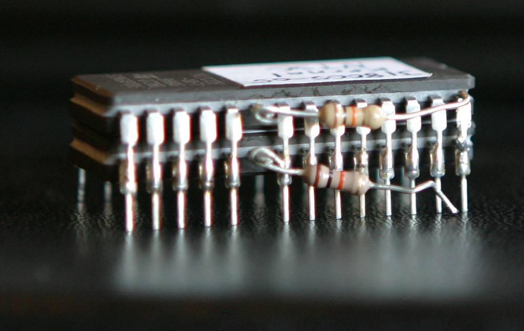
| After soldering the resistors onto the chips, they are placed together just on top of the socket so that the wires connecting to the switch can be routed and trimmed. |
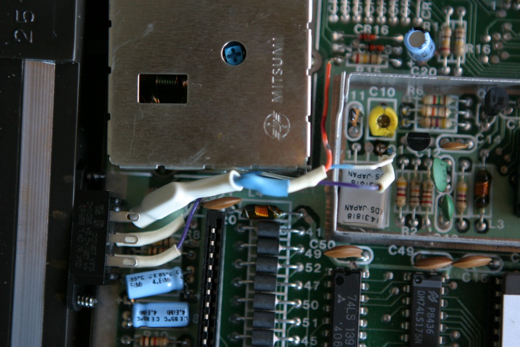
| The last step is to wire up the top pole of the switch, to select between the two EPROM chips. Pin 20 of the bottom (PAL) EPROM should be wired to the top switch lug which is closest to the back of the computer. The middle lug of the top pole on the switch should be connected to ground. I used the nearby big solder blob on this machine. The bottom lug of the switch (closest to the user) should be connected to pin 20 of the NTSC (top) EPROM. |
| There are seval improvements which can be made to this mod. I should have used heat shrink on the top pole switch lugs as well as the bottom. More importantly, the second kernal EPROM chip interferes with the metal plate under the keyboard. The case can be closed and screwed shut even with the extra EPROM, but the circuit board will have to bend a millimeter or so to accomodate. A better design for the kernal ROM switch is to use a single bigger (27C256 32k) EPROM and select between the halves of the ROM space (using the A14 line on pin 27), instead of using two 16k EPROM chips. This will also be easier to build, as the pull-up resistors on the chips won't be necessary. |
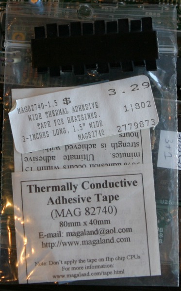
| I decided to also add heatsinks to the CPU and TED chips, with the hopes of extending their lives. I had some thermally conductive tape sitting around which was purchased at Fry's long ago: |
| For heat sinking these chips, you have very little vertical room to work with. For the CPU (8501, on the right), I used the top part of an NTE448G 40-pin DIP clip-on heatsink, and attached it to the CPU with the thermal tape. For the 8360 TED chip, I took two TO-220 heat sinks and bent over their fingers to lie flat. |
| That's it. The mod works perfectly, and I am able to run in either PAL or NTSC mode. |
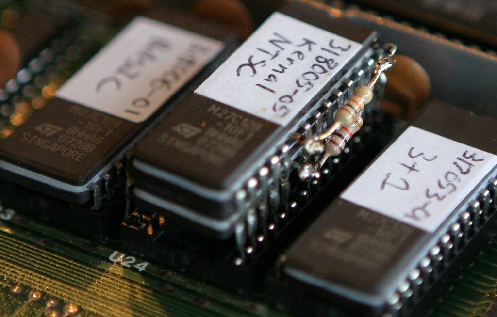
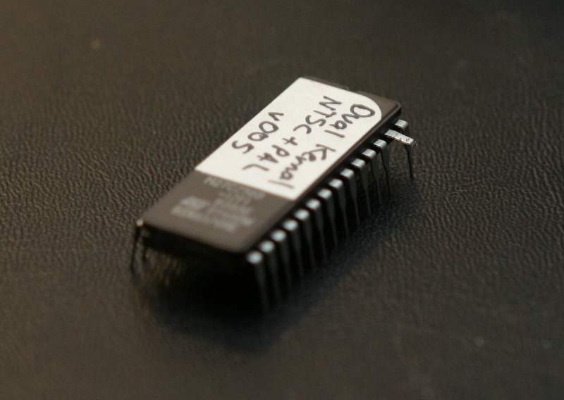
| I decided to improve the mod on this machine in order to address the issues that I mentioned above. I started with a 27C256 EPROM (32k), which has the same number of pins and nearly the same pinout as the 27C128s originally used in the Plus/4. First I burned this ROM with the NTSC kernal image in the bottom half of the memory space, and the PAL kernal image in the top half. Then I bent pin 27 outward and trimmed it off as shown here: |
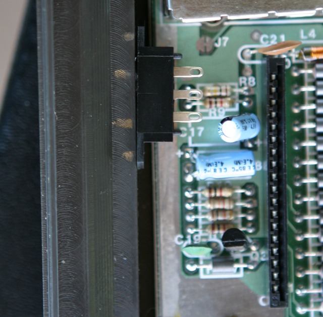
| Then I re-wired the top pole of the DPDT switch. The terminal closest to the user goes to ground, while the terminal away from the user must be connected to a +5 volt source. I used the rightmost solder pad for the small inductor labeled L4. This time I remembered to cut small pieces of heat shrink tubing and slip them around the wires before soldering both ends. |
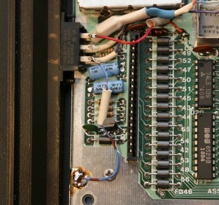
| Then I trimmed the leads of a 10k resistor very short and soldered it to the center terminal of the top pole. I soldered a piece of hook-up wire to the end of the resistor, and routed the other end to pin 27 of the EPROM. The 10k resistor isn't really necessary in this circuit but it will protect things in case the pin 27 is accidentally shorted to ground. |
| And this is what it looks like with everything routed and shrunk: |
| I'm very happy with the mod now. It works perfectly and the case closes with no problem. |